

The effort to relocate semiconductor manufacturing to the United States, which Washington has been betting on for several years, may not be as effective as the authorities had hoped. So far, billions of dollars have been allocated to the construction of advanced factories, one of the most critical stages in the modern semiconductor manufacturing process. However, advanced chip packaging remains almost entirely dependent on Taiwan. Amid the AI boom, this segment is rapidly becoming a new strategic asset, while packaging shortages are emerging as a potential bottleneck for the industry’s future growth.
The administration of Donald Trump refused to finance the creation of a research center for the development of advanced chip packaging technologies in Arizona, although under the previous administration, it was planned to allocate $1.1 billion for this project. After the cancellation of funding, the non-profit organization that was supposed to manage the center effectively ceased to exist.
This decision has only increased the dependence of the American semiconductor industry on Taiwan’s TSMC. Beyond chip fabrication itself, packaging technology is the second most important element of the modern semiconductor industry, while the US supply chain in this area remains even more vulnerable than in the wafer segment.
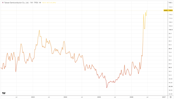
Historically, American companies have paid little attention to chip packaging, so today the US share of the global market for such services does not exceed 3%. Meanwhile, the development of artificial intelligence has dramatically increased the importance of this stage of production. Modern AI accelerators consist of several computing chips and HBM memory stacks combined on a single substrate. Without advanced packaging methods, building such solutions becomes impossible.
CoWoS technology is currently the industry’s most widely used advanced packaging technology and is used for Nvidia’s accelerators. However, demand is so high that, according to market participants, the Taiwanese company’s production facilities are already estimated to be about 30% below customer needs. At the same time, the cost of packaging can reach $500 for the most complex chips, significantly increasing their cost. That is why some developers deliberately choose simpler layout options, trying to reduce costs.
Even the construction of new TSMC facilities in Arizona has not solved the problem yet. Until U.S. packaging facilities begin operating — currently expected in 2028–2029 — U.S.-made silicon wafers will still have to be shipped to Taiwan for final packaging and testing.
Despite the lack of large-scale government support, private investment in this segment continues to grow. Intel and Applied Materials are independently expanding their core capacities in the United States, and Amkor Technology is preparing to invest at least $7 billion in the construction of its first American advanced chip packaging facility. It is already known that Apple, Nvidia, and TSMC itself are showing interest in partnering with the company.
At the same time, new alternatives to TSMC are also appearing on the market. One of Intel’s most notable customers is Taiwan’s MediaTek, which will now be able to use packaging technologies from two of the industry’s largest players at once. The company is becoming one of the few that has access to both TSMC’s and Intel’s advanced packaging capabilities. This is of strategic importance as demand for modern packaging technologies continues to grow rapidly alongside the expansion of AI infrastructure.
This could be especially important for Intel, whose stock declined at the beginning of July, weakening the company’s position on the heatmap. According to Nikkei, MediaTek is working with Google to develop custom artificial intelligence accelerators that can use proprietary EMIB packaging technology. If the project is implemented, Intel will receive a major order for its contract division, which has yet to become profitable.
MediaTek itself expects to capitalize on the AI boom. Already this year, the company plans to generate about $2 billion in revenue from AI server chips and expects to exceed this figure next year. At the same time, production of advanced processors will remain with TSMC, which is already supplying MediaTek with prototypes of its future 1.4 nm chips.
TSMC’s international expansion continues in parallel. The first 4 nm chip manufacturing facility is already operating in Arizona, the second is preparing for equipment installation, the third is under construction, and the creation of the first American packaging and product testing facility is beginning. In addition, the company is expanding production in Japan and Germany, bringing chip production closer to key customers.
As a result, packaging is gradually becoming one of the scarcest resources in the global semiconductor industry. If a few years ago advanced process technologies were considered the main competitive advantage, today the ability to quickly and efficiently combine computing chips, memory, and other components into a single system is becoming just as important. And while the United States is investing tens of billions of dollars in localizing chip production, dependence on Asian advanced packaging capabilities remains one of the biggest strategic vulnerabilities for the U.S. semiconductor industry.